Rescuing a T23 NOR with a CH341A and an SOP-8 clip
When the USB cloner can still read but can no longer write through the SoC SFC, stop retrying the broken master — clip the flash, dump first, then erase, program, and verify off-board.
The diagnosis that forces this tool is already written in Debugging an SFC failure with Vibe Coding: two identical cloner readbacks, image match only through 0x99F, a foreign xboot from 0x9A0, erased 0xFF from 0xC000. The USB cloner can still talk to the chip through the SoC for long enough to prove the write path is dead. Another stage2_write is not a method.
This note is the bench procedure that follows — a CH341A programmer and an SOP-8 test clip on the 16 MB NOR itself, with the Ingenic T23 not running as a second SPI master.
1. What you are buying
About fifteen to twenty-five yuan of hardware, and a Windows tool that unpacks without an installer.
| Item | Notes |
|---|---|
| CH341A programmer | The SPI/I2C programmer brick, not a bare serial adapter |
| SOP-8 test clip | Usually bundled; eight springs for the NOR package |
| Ribbon cable | Clip → programmer, eight wires |
Software on this pass: NeoProgrammer 2.2.0.10. It identified the FM25Q128 and read SPI ID A14018 cleanly. CH341A Programmer v1.4 and flashrom are backups, not the first move.
2. Driver, then the right header
Plug the CH341A in. Install the CH341A PAR driver (CH341PAR.EXE from the vendor zip, or Zadig). Device Manager should show something like USB-EPP/I2C ... CH341A. The serial CH341 driver is the wrong stack for this job.
On the brick, silk splits the header into BIOS 25 SPI and EEPROM 24 I2C. The green adapter and ribbon sit on the 25 SPI side only. The I2C half looks adjacent and will waste an afternoon. Leave the jumper on 1-2 (编程 / programming), not TTL.
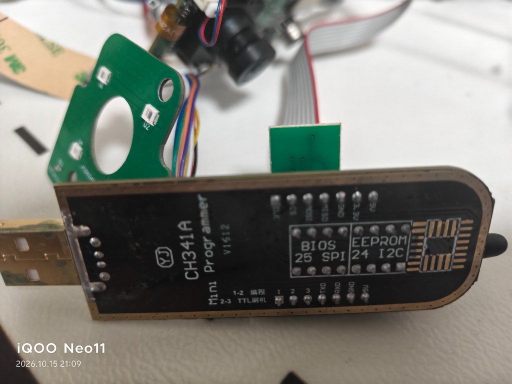
Adapter on BIOS 25 SPI, not EEPROM 24 I2C. Pin labels (CLK / CS / MOSI / MISO / GND / 3.3V) face the SPI row; jumper stays on programming.
3. Product power off, then clip pin 1
The part on this board is a FM25Q128-class 16 MB NOR in SOP-8. Pull battery and product USB so the MCU cannot raise the T23 rail. The CH341A will still feed 3.3 V through the clip; board power LEDs lighting up is expected and is a contact check, not “the SoC is on.”
Pin 1 is the notch (or the silk dot). With the notch to the left (top view):
        +--U--+
  CS# --|1   8|-- VCC
  MISO--|2   7|-- HOLD# (usually tied high in the clip)
  WP# --|3   6|-- CLK
  GND --|4   5|-- MOSI
        +-----+
Red stripe / marked pin 1 on the ribbon and clip aligns with chip pin 1. Reverse polarity usually fails to identify; it should not fry the part — but it also does not dump anything useful. Seat the clip firmly before you trust a read.
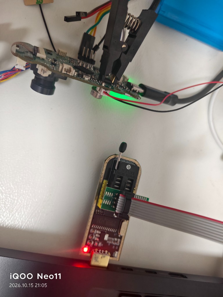
Clip on the NOR, red-stripe ribbon to the CH341A. Programmer red LED and board green LED on: clip VCC is reaching the flash. Product battery/USB still stay out.
4. Identify, then read — keep the dump
Open NeoProgrammer. Detect, or pick FM25Q128 (GD25Q128 / W25Q128 are often compatible stand-ins if the ID is close). A live SPI ID is the first software proof that the clip, header, and power are right.
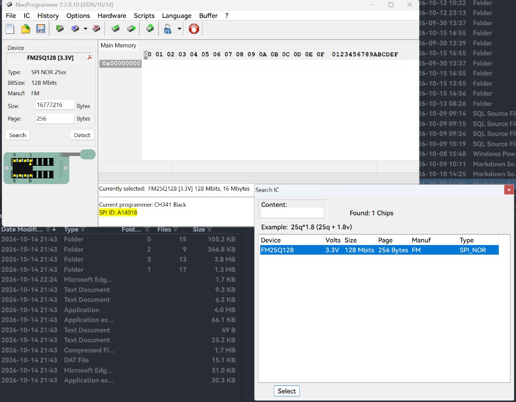
NeoProgrammer 2.2.0.10: programmer = CH341 Black, device = FM25Q128 [3.3V] 16 MB, SPI ID A14018. That ID is the contact check in software.
Then forensics before rewrite:
- Read — on the order of one to two minutes for 16 MB.
- Save the buffer before you erase anything.
- Diff the dump against the image you thought was on the chip. The cloner story (prefix match, foreign xboot,
0xFFhole) should show up again here if the SFC read path had been telling the truth.
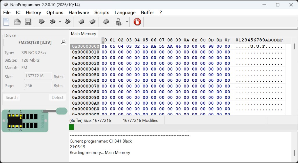
Read in progress / complete: buffer size 16,777,216, hex at 0x00000000 already non-empty (06 05 04 03 02 55 AA …). Save this buffer before Erase.
A dump you never open is still cheaper than an erase you cannot undo.
5. Erase, program, verify — in that order
Use a known-good full image. On this project the delivery blob is on the order of 14 MB into a 16 MB part; check length and a hash before you click Program. Buffer base address stays 0x000000.
- Erase chip — real erase takes on the order of a minute or two. A one-second “erase” in the USB cloner was one of the original red flags; do not trust a flash of green here either until the buffer shows
0xFF. - Open the firmware file into the buffer.
- Program — several minutes.
- Verify — must pass. Fail means erase-and-retry once; fail again means the die itself, and a heat-gun swap of the FM25Q128, not another SoC cloner profile.
Keep product power off for the whole sequence. Unplug the CH341A (or disconnect in software) before you lift the clip.
That is the end of the clip job: the NOR matches the file. Serial banner, cmdline, and a real recording after power-on are the next bring-up story — not this procedure.
6. Two outcomes after Verify
| External verify | Board after clip | Meaning |
|---|---|---|
| Pass | Boots and brings up cleanly | The NOR was the patient. Retest a short on-board program later; do not assume the SFC path is healthy forever. |
| Pass | Still dead | The image is on the chip. The remaining fault is the SoC SFC pins or address path — rework or another board, not another cloner profile. |
| Fail after re-erase | — | Flash die is bad. Replace the package. |
7. What the October board looked like before the clip
Not folklore — the record that justified leaving the SoC path:
- Cloner fake-erase (~1 s), then write die at 1–5% with
stage2_write error(-1)four times, thenPERM ERR. - Eight good programs the same night; after one later image ran about ten minutes, every subsequent program failed.
- Ruled out first: image bytes, MCU firmware rollback, radio quiet, full battery.
- Cloner read strategy:
0x000–0x99Fmatched the intended image; from0x9A0a different xboot build; from0xC000erased0xFF; two readbacks byte-identical.
That is when the shopping list above stops being optional.
8. Keep these rules on the sticky note
- Product rails dark while the clip owns SPI. Programmer VCC through the clip may light LEDs; that is fine. Battery and product USB are not.
- Pin 1 and the SPI header before any erase. No SPI ID almost always means wrong orientation or the I2C half of the brick.
- Dump before erase. Forensic first, rewrite second — save the 16 MB buffer while it still exists.
- Verify closes the clip. Board bring-up after that is a separate note.
- Stop programming through a master you have already shown cannot write. The clip is the next experiment, not the seventh cloner retry.
The cheap programmer does not replace judgment about which bus master is broken. It only gives you a bus master that is not the one that already failed.
Questions this note answers
When is a CH341A clip the right next step?
After cloner readback shows a deterministic partial image — a clean prefix, a foreign xboot splice, then a hole of 0xFF — and the same image fails through the SoC. Another cloner profile will not heal a write path the SoC has already lost.
Why must the board stay powered off while the clip is on the NOR?
The T23 SFC and the CH341A would both drive CS, CLK, and the data lines. Two masters on one SPI bus make the dump and the program untrustworthy. Pull battery and product USB before the clip attaches. The programmer’s own 3.3 V through the clip may light board LEDs — that is contact power, not a second master.
What closes the CH341A job?
NeoProgrammer Verify must pass against the image you meant to write. Whether the board then boots is a separate bring-up question — serial banner, cmdline, and recording belong in that story, not in the clip procedure.